Synthesis and Pin Assignments
Now that the design has been entered we will translate the written design into a form that is machine-readable. For SoCs, this process is called synthesis. Before the synthesized design is placed into a device we will also set up the design constraints. For this tutorial, the only constraints we will place are the pin assignments.
| It is quite common for a designer to perform a function simulation of their designs prior to synthesis. For this simple example, we are omitting the simulation step |
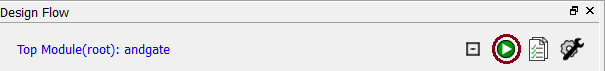
1) Double-click Synthesize under Implement Design in the Design Flow window to synthesize the design with Synplify Pro. Synplify Pro adds I/O pads to the design. A green check mark appears in the Design Flow window to indicate synthesis was successful

Since this is a very simple design, the only other thing we need to do is tell the tools which I/Os to use. Double-click Manage Constraints in the Design Flow window to open the Libero SoC Constraints Manager.

3) Confirm the I/O Attributes tab is selected. Use the pull-down menu on the Edit button to select Edit with I/O Editor (highlighted in the figure above) to open the I/O Editor.
4) Select the Port View tab of the I/O Editor.
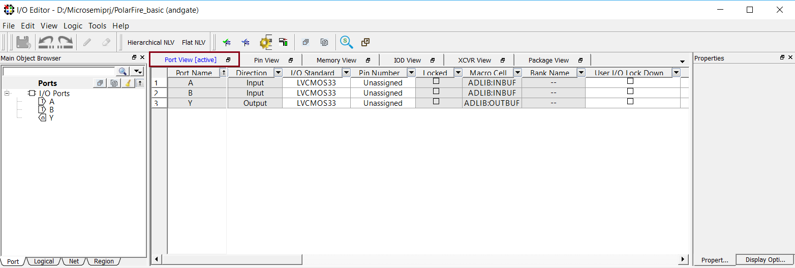
5) Use this window to set the I/O Standard and Pin Number. Confirm that LVCMOS33 is the I/O Standard for each pin.
6) Click Unassigned in the Pin Number column to reveal available I/O pins. Make the following assignments: (you can type the pin number in the field or use the pull-down menu to select the pin)
- A -> K5
- B -> K4
- Y -> P7
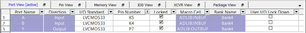
7) Make sure your connections match the image below then click on File > Commit and close the window, File > Exit.
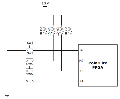
Push-Button Switches
The PolarFire Splash Kit comes with four debug push-button switches that are connected to the PolarFire FPGA. The table below lists the onboard push-button switches.
| Switch Number | FPGA Pin Number | FPGA Pin Name |
|---|---|---|
| SW3 | L6 | GPIO210PB4 |
| SW4 | M7 | GPIO210NB4 |
| SW5 | K5 | GPIO211PB4/DQS |
| SW6 | K4 | GPIO211NB4/DQS |
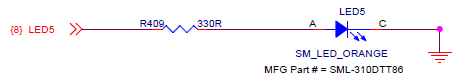
User LEDs
The board provides user access to eight active low LEDs, which are connected to the PolarFire device for debugging applications. The table below lists the onboard debugging LEDs.
| Reference Board LED | FPGA Pin Number | FPGA Pin Name |
|---|---|---|
| LED1 | P7 | GPIO186PB4 |
| LED2 | P8 | GPIO186NB4 |
| LED3 | N7 | GPIO187PB4/DQS |
| LED4 | N8 | GPIO187NB4/DQS |
| LED5 | N6 | GPIO188PB4 |
| LED6 | N5 | GPIO188NB4 |
| LED7 | M8 | GPIO189PB4 |
| LED8 | M9 | GPIO189NB4 |
8) If you click the green arrow button at the top of the Design Flow window, you can now run the design all the way through Place and Route. This will apply the constraints to the synthesize, then place the netlist on the device and route the interconnections.