PID Basics: dsPIC® DSC Implementation Part 2
dsPIC® DSCs Implementation Operations
The first operation is to set the two pointers to point at the first location of each buffer in the RAM. In the following diagram, W8 is the pointer to the coefficients buffer; W10 is the pointer to the error buffer.

The new error value is computed as the difference between the reference voltage (Vref) and the new output voltage read by the ADC (ADCBUF1). See figure below.

movsac Instruction
The movsac instruction performs a number of different tasks. The following diagram and steps demonstrate the movsac instruction.

1) Move RAM contents
1a: Moves the content of the RAM location pointed to by W8 into register W4.
1b: Moves the content of the RAM location pointed to by W10 into register W5.

2) Update Working Registers
2a: Updates the W8 register, so that it is now pointing to the following RAM location.
2b: Updates the W10 register, so that it is now pointing to the following RAM location.


PID term computation
Below are the computation steps of the first term of the PID:
1) The W4 and W5 registers' contents are multiplied and the result is added to the 40-bit accumulator B.

2) Moves the content of the RAM location pointed to by W8 into register W4.
3) Moves the content of the RAM location pointed to by W10 into register W5.

4) Updates the W8 register, so that it is now pointing to the following RAM location.
5) Updates the W10 register, so that it is now pointing to the following RAM location.
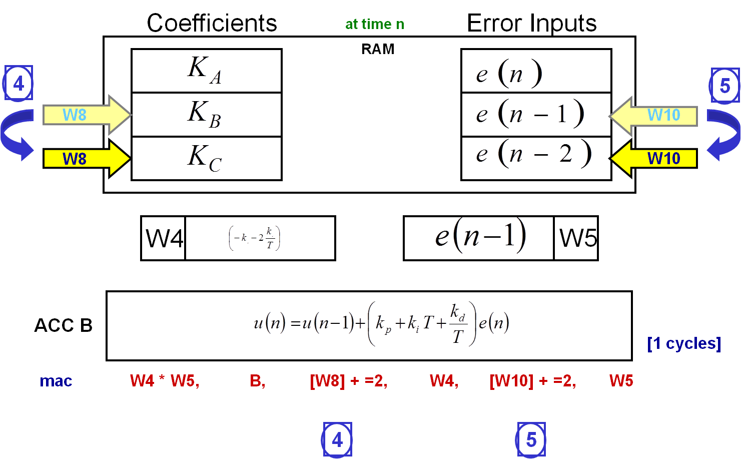
6) The W4 and W5 registers' contents are multiplied and the result is added to the 40-bit accumulator B.
